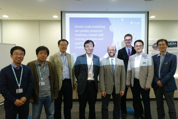

Dr Simon Elliott, Head of Group - Materials Modelling for Devices, gave an invited seminar on simulating Atomic Layer Deposition (ALD) at Samsung Semiconductor R&D Center, Hwaseong, Seoul, Korea on 14 October 2016.
Dr Elliott was hosted by Master HanJin Lim, as part of a joint visit with Dr Dennis Hausmann of Lam Research.
Atomic layer deposition or ALD is a method which does exactly what it says, depositing materials essentially one atomic layer or less at a time. Although it is a relatively slow process, since it is controlled by what are termed self-limiting surface reactions it is capable of highly conformal deposition that follows the often complex contours of the substrate resulting in a layer which is extremely uniform in thickness. ALD is now routinely used in the electronics industry. However, ALD is now also becoming increasingly important for other areas such as solar energy, medical devices and packaging.
