Leader in Integrated ICT Hardware & Systems
The objective of SP&S is to cater for all customer needs, and to substantially increase industrial revenues while continuing to develop leading edge process technologies and devices in collaboration with Tyndall researchers.
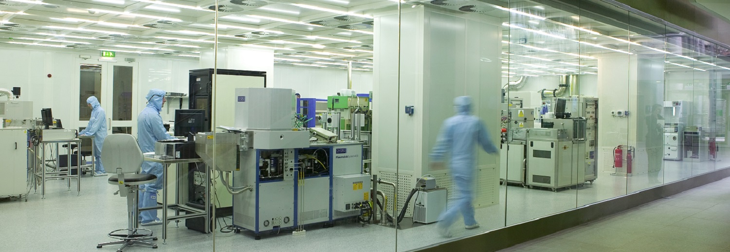
The centre comprises frontend activities encompassing cleanroom fabrication and training facilities as well as back-end Device Forensics activities including analysis, test, reverse engineering, packaging and reliability.
Our flexible fabrication offering - FlexiFab - is in a unique position to allow for greater material exchange between the fabrication areas, whilst maintaining protocols to avoid cross contamination. The flexible exchange of materials and devices on offer here across the functional areas of CMOS, MEMs and Compound Semiconductor is unique in industrially accessible fabrication facilities. This enables the type of material integration essential for the More than Moore and IoT domains, where advanced sensors are made network aware. Our extensive ‘back-end’ facilities and expertise enable us to take the resulting functionalised devices and package them in a form that enables the customer to use them in their real world systems. Coupled with this are capabilities in reliability testing, reverse engineering, electron microscopy and analysis which together provide the diagnostic tools that allow for the forensic analysis of materials and devices.
Tyndall’s extensive fabrication facilities cover:
The flexible fabrication facility enables the heterogeneous integration of materials advanced device development. This enables the type of material integration which is essential for the More than Moore and IoT domains where advanced sensors are made network aware.
The resulting functionalised devices are transferred into the Device Forensics area for packaging, analysis, reliability and test.
Complementing the ‘front-end’ fabrication capabilities, Tyndall has extensive ‘back-end’ facilities and expertise to be able to take the functionalised devices and package them in a form that enables the customer to use them in their real world systems. Married with this are capabilities in reliability testing, reverse engineering, electron microscopy and analysis which together provide the diagnostic tools that allow for the forensic analysis of materials and devices.
The particular capabilities cover the areas of:
Contact enquiry (at) tyndall (dot) ie for all Business Development enquiries