Process & Product Development
It encompasses:
- Silicon fabrication
- MEMS or microsystems fabrication
- Compound semiconductor fabrication
- E-beam lithography
- Training facility
- Circuit device and structure layout.

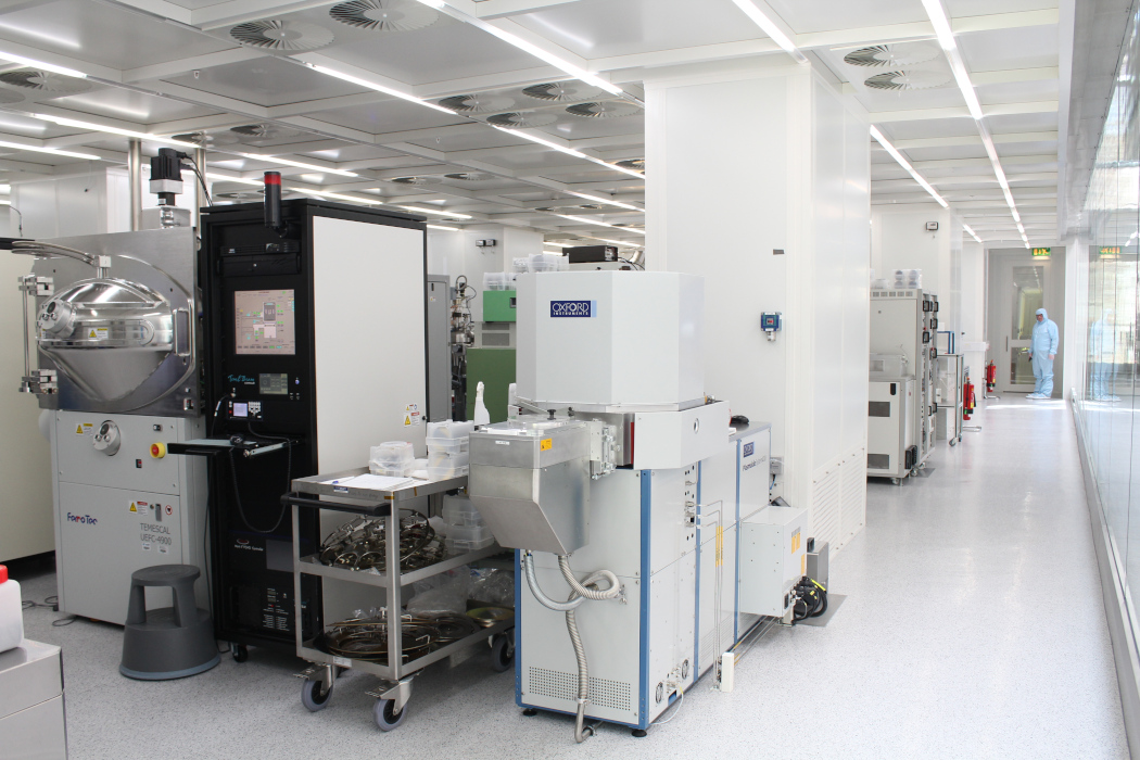
All of Tyndall’s cleanroom facilities are compatible with 100mm substrates. A number of newer tools are either 200mm compatible or upgradeable if the need arises. The fabrication facility is fully integrated with other key elements within Tyndall such as packaging, design, test and characterisation, electron microscopy and analysis. This provides our customers with a complete service solution from concept to circuit design, through to fabricated device, and packaged tested system.
One of the key attractions in working with the P&PD group is the degree of process flexibility which we offer. The availability of the different process lines allows us to define routes whereby often incompatible materials (for example, gold in a CMOS line) can be brought together within the same facility and cross-contamination avoided through tool and protocol separation. This allows the integration of these different materials with their own unique properties to deliver the prototype or product with the unique attributes required by our customers.
The cleanrooms are also home to a number of commercial companies that use our facility to carry out process development and pilot production and that are able to leverage the support of the process expertise within P&PD to de-risk and accelerate their product development.

Fabrication Laboratories
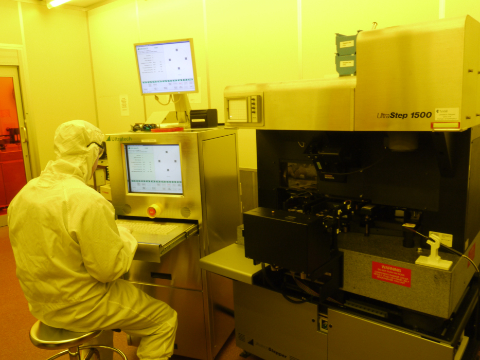
The Silicon fabrication laboratory is configured to run 100mm substrates and maintains a CMOS-compatible line. While offering a variety of full processes (CMOS – 5um and 1.5um), Silicon PIN diodes and PMOS RADFETs, it also offers the following technologies: wafer cleaning, thermal treatments, photolithography, plasma etching, plasma deposition, PVD and ALD.
In the MEMS fabrication laboratory we have capability and expertise in polymer processing, photolithography, wafer bonding, bulk micromachining, plasma etching, mixed frequency plasma deposition and metal deposition. Silicon microneedles fabrication and magnetics on silicon device processing are two specific areas of interest in our MEMS lab.
In the Compound Semiconductor fabrication laboratory, research work primarily focuses on the fabrication of photonic devices on substrates comprising of Gallium Arsenide (GaAs), Gallium Nitride (GaN), Indium Phosphide (InP) and alloys. Our fabrication staff provide process support to the research activities by developing new processes in the areas of plasma etching and dielectric deposition as well as providing process expertise in the core areas of photolithography, metal evaporation, dielectric coating, sputtering, plasma deposition and etching.