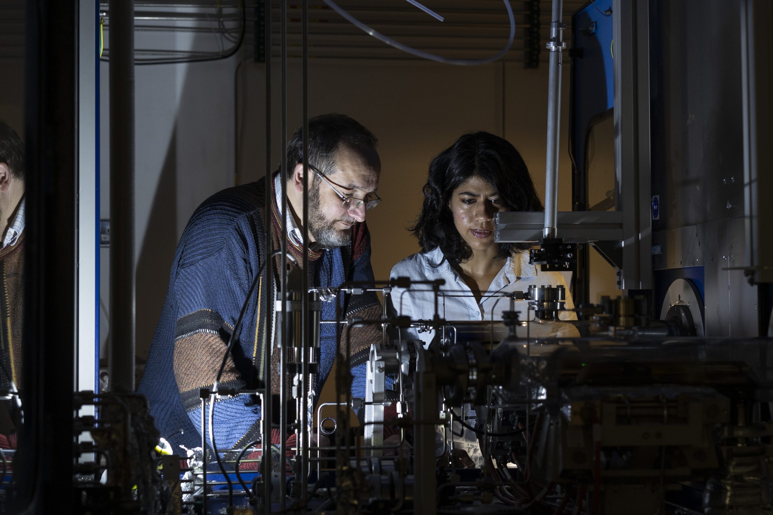
Tyndall’s Quantum photonic teams contribute to our evolving “Quantum Technology” research programme. The programmes encompasses the direct development and implementation of quantum light sources (including both the materials choice and device design e.g. developing quantum dot sources) – their theoretical understanding through computational modelling and the development of hybrid integration schemes for enabling devices capable of providing “on chip” solutions to the world quantum computing effort, availing of Tyndall’s fabrication capability in its state-of-the-art cleanroom facilities.
Our vision is to enable deep-tech innovation for emerging quantum photonic technologies, specifically focusing on quantum information processing and telecommunications (and sensing).
Our mission is to deliver state-of-the-art solutions to obtain:
- The development of semiconductor “artificial atom” concepts (e.g. quantum dots and similar) and devices tailored to be efficient quantum light sources (e.g. entangled light)
- Enhanced photonic hybrid on–chip capabilities for quantum signal processing, computation and sensing
- The development of advanced packaging solutions to enable real life device demonstrators for emerging photonic quantum technologies (from cryptography to computation).

Research Challenge
There are several research challenges which are key to the development of next generation quantum photonic devices. Firstly, there is the understanding of epitaxial processes necessary to develop the required nanostructures and planar devices. Secondly, technological challenges require the development of new architectures and novel material ensembles, beyond the simple single nanostructure concept and towards complex devices, merging the potentiality of different material platforms, e.g. from semiconductor to polymer assemblies.
These developments need to go hand in hand with the emerging field of large-scale photonic integration, from hybrid integration challenges to enable on chip photonic computation, to developing photonic packaging solutions compatible with the harsh (typically cryogenic) environments photonic chips are intended to operate in.
Research Focus
Our research focus is organised around frontier research in materials development, their organisation and device structure modelling, the development of hybrid integration concepts for on-chip photonic quantum information processing (specifically for harsh cryogenic applications) confirmed by proof-of-concept device demonstrations.
Recent Publications
E. Pelucchi, G. Fagas, I. Aharonovich, D. Englund, E. Figueroa, Q. Gong et al, “The potential and global outlook of integrated photonics for quantum technologies” Nature Reviews Physics, 4(3), 194-208, (2022).
E. Pelucchi, S. T. Moroni, V. Dimastrodonato, D. D. Vvedensky,
“Self-ordered nanostructures on patterned substrates: Experiment and theory of metalorganic vapor-phase epitaxy of V-groove quantum wires and pyramidal quantum dots“, Journal of Materials Science: Materials in Electronics, 29, 952-967, (2018).
S. K. Patra and S. Schulz, “Indium gallium nitride quantum dots: consequence of random alloy fluctuations for polarization entangled photon emission.” Materials for Quantum Technology, 1 (1) (2020).


