Advanced Photonic Packaging Research
Advanced packaging is now the key technological driver for the next generation of semiconductor systems, fulfilling the massively increasing demands for high performance, power efficiency, small form factor and low-cost packages across multiple industry market sectors.
However, many technical challenges remain, from the fundamental scientific challenges of more advanced, reliable and sustainable packaging materials, cost-effective package designs and packaging process flows, to the engineering challenges of package design standardisation and process automation for high-throughput manufacturing.
Through the Photonics Packaging and Systems Integration research programme at Tyndall, we address these challenges, spanning fundamental research to pilot-scale manufacturing.
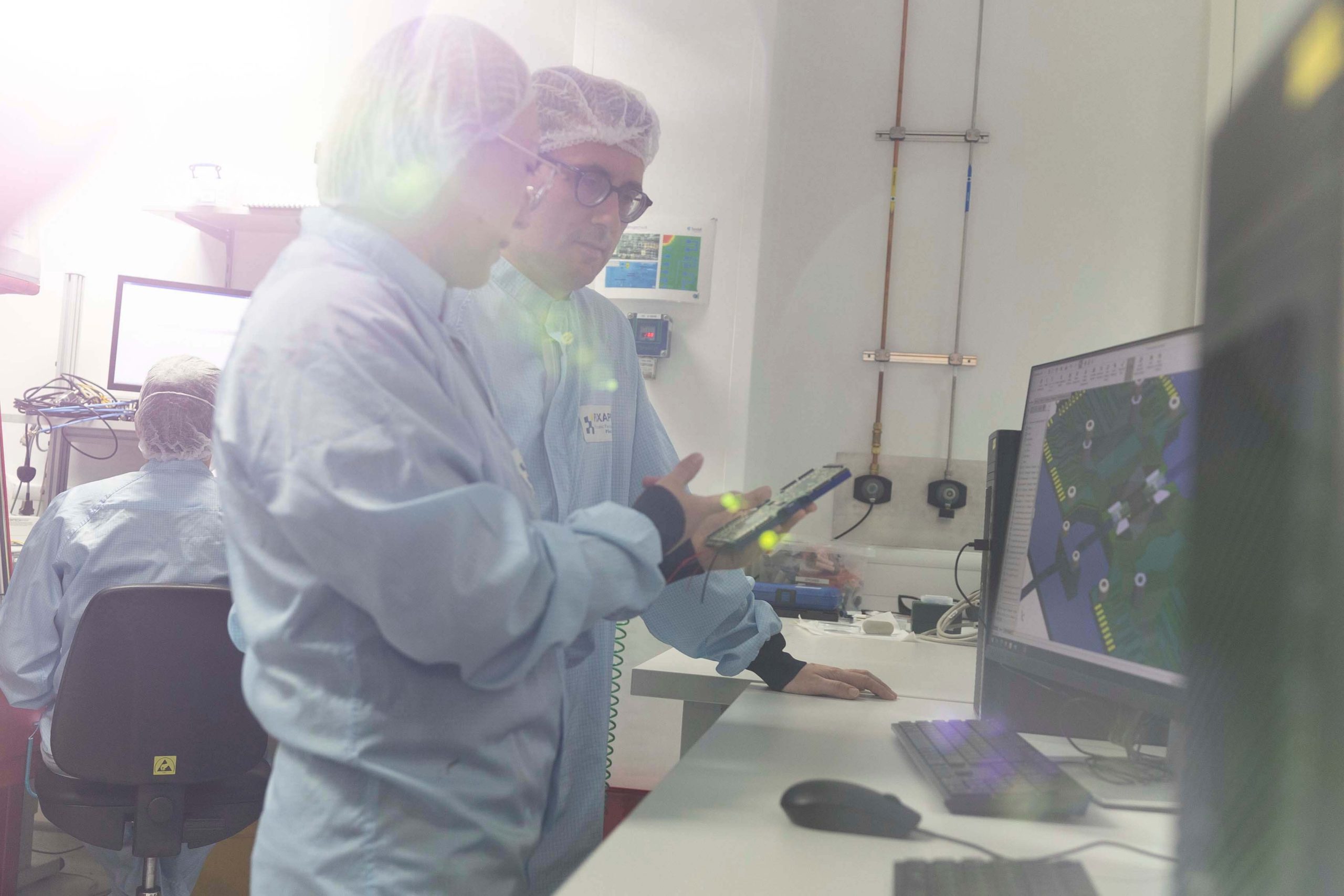
The team consists of highly skilled and dedicated researchers, engineers, project managers and PhD students. Led by Prof. Peter O’Brien, we have unique technical expertise in advanced photonic and microelectronic packaging and integration technologies.
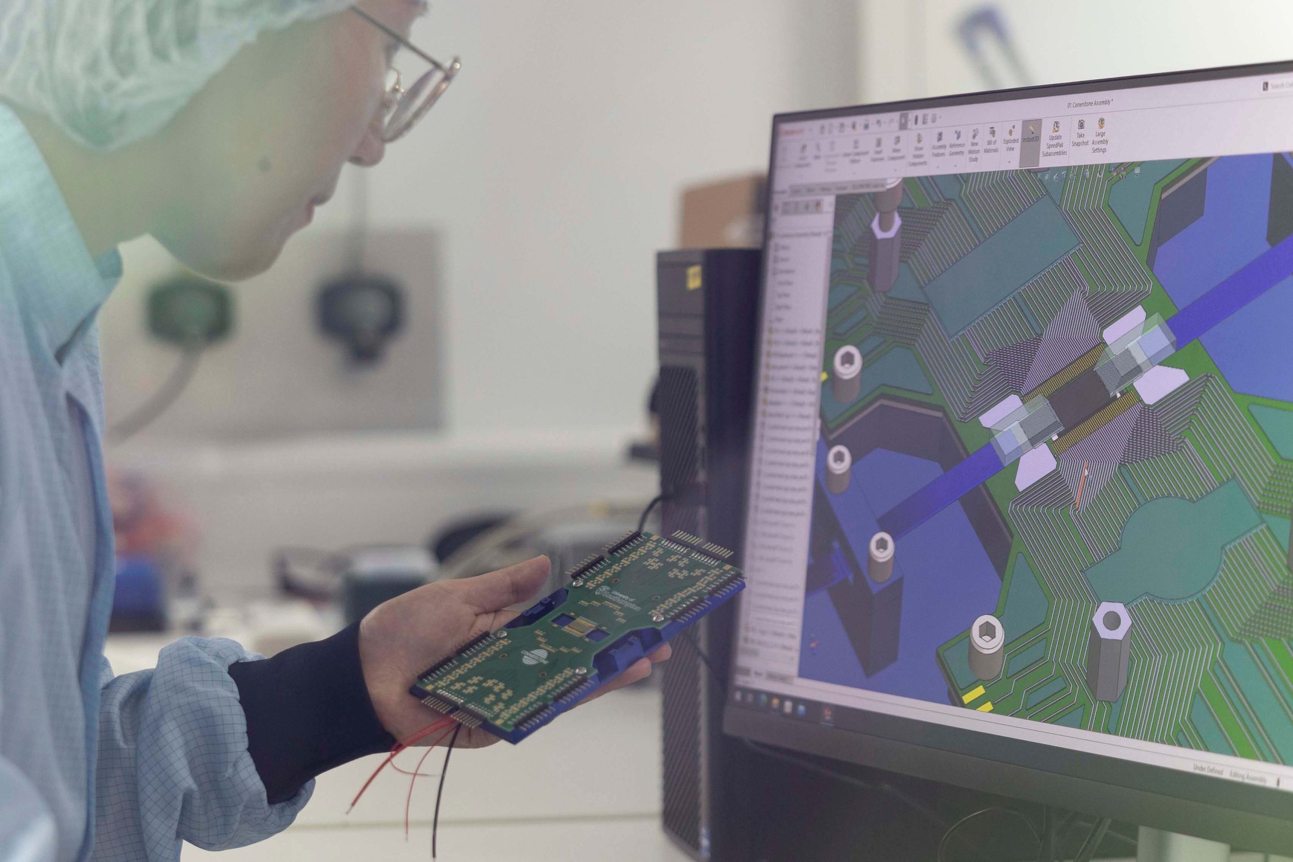
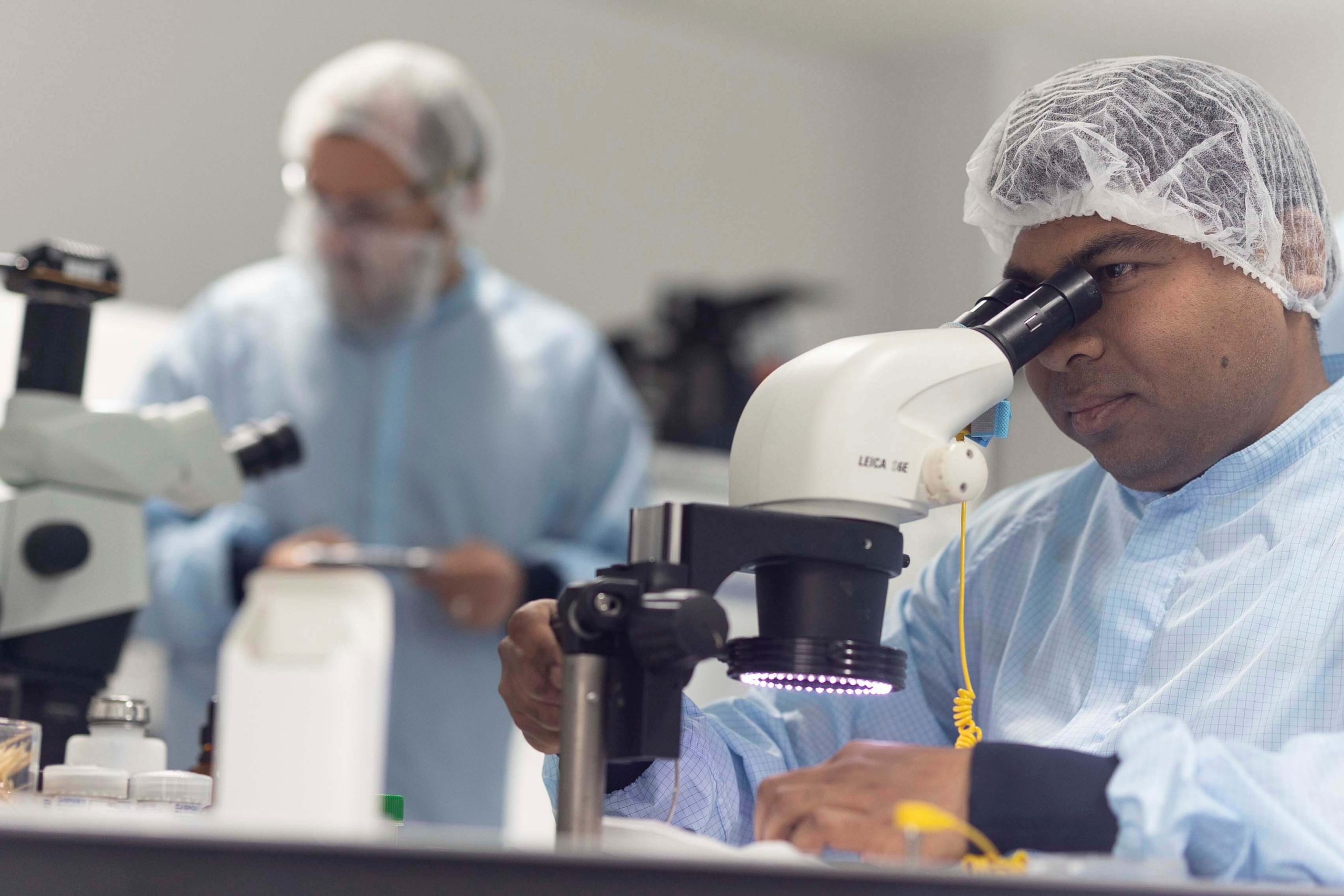
With state-of-the-art front-end and back-end facilities, we specialise in developing novel optical coupling, laser and electronic integration technologies, focusing on wafer-scale packaging for scale-up to volume manufacturing.
We have a long-term vision centred on delivering world-class research focusing on 3D photonic-electronic chiplet systems, which presents some of the toughest packaging challenges we know. We strive to advance the field from fundamental research to practical applications, contributing to the growth of photonic and microelectronic technologies in Europe and worldwide.
We collaborate with multiple academic and industry groups worldwide and are a lead partner in major research programmes including:
- European Photonics Packaging Pilot Line – PIXAPP
- Europractice
- PhotonHub Europe.
We also collaborate with leading photonic equipment manufacturers including:
- ficonTEC
- X-Celeprint.
Collaboration with leading photonic equipment manufacturers like ficonTEC and X-Celeprint enhances our capabilities, positioning us at the forefront of innovation in high-throughput photonic-microelectronic manufacturing. These international collaborations are developing next-generation solutions for high-throughput photonic-microelectronic manufacturing.
Research Focus
We are dedicated to addressing global challenges in photonic and microelectronic technologies. Our innovative solutions span diverse applications, including high-speed communications, healthcare diagnostics, biosensing and others.
We address societal challenges through advancements in photonic packaging. Our innovative solutions impact high-speed communications, healthcare diagnostics and emerging markets like the Internet of Things and LiDAR. By focusing on 3D photonic-electronic chiplet systems, we contribute to improved communication systems, more efficient healthcare diagnostics, and the development of compact solutions for IoT applications. Through global collaborations, we actively shape the future of photonics and microelectronics.
By leveraging our unique expertise and state-of-the-art facilities, we develop advanced prototypes and manufacturing routes, contributing to the evolution of communication systems, medical technology, remote sensing capabilities, and emerging technologies like quantum computing. Our focus on 3D photonic-electronic chiplet systems reflects a long-term commitment to advancing packaging and integration technologies.
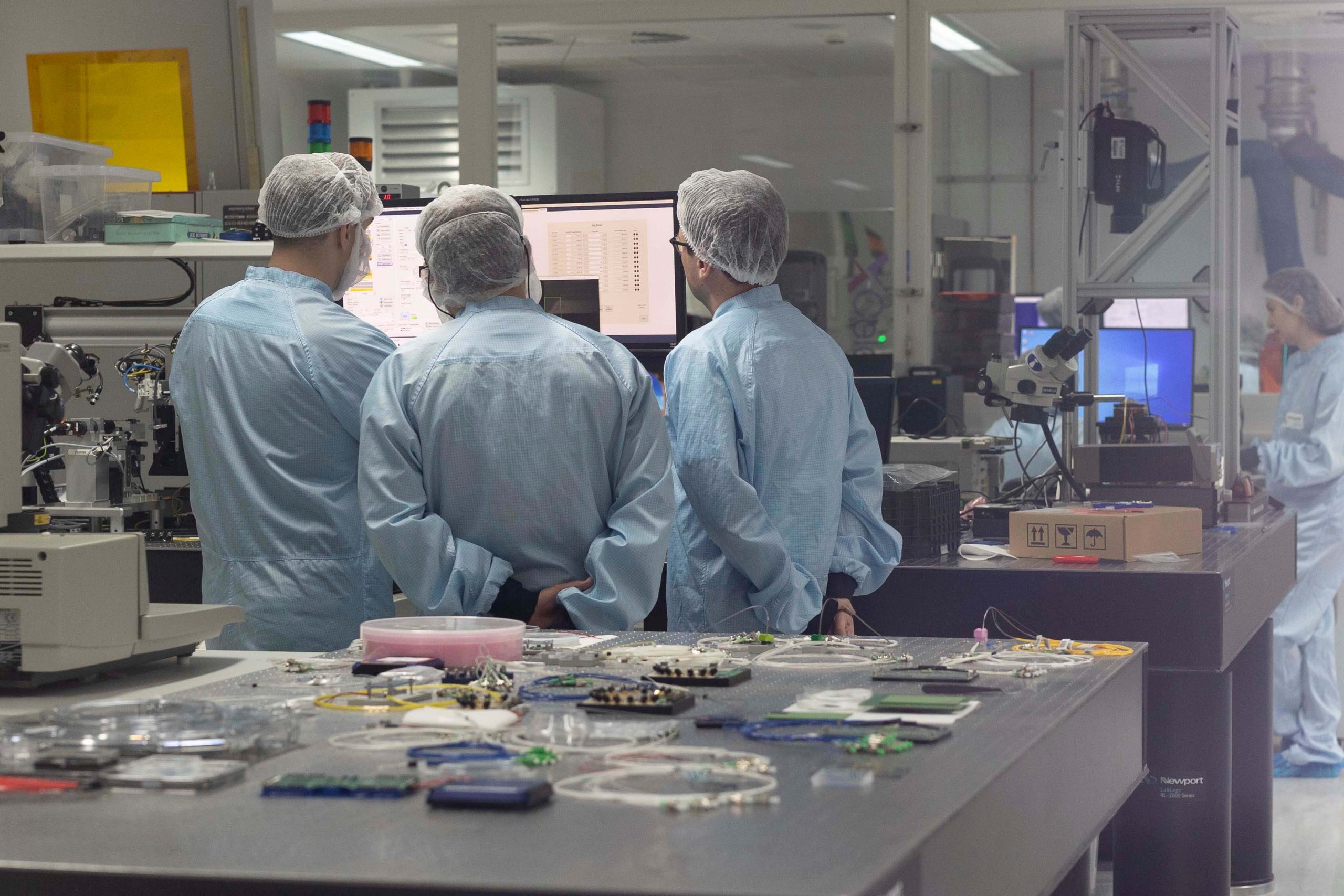
The cutting-edge facilities encompass simulation, design and production capabilities, utilising state-of-the-art equipment from prototype development to low-volume production. Through active participation in global initiatives and collaborations with leading manufacturers, we address current challenges and contribute to shaping the future of photonics and microelectronics.
We actively address challenges in wafer-level packaging, RF photonic-electronic integration, quantum photonics, and more, contributing solutions to global issues in communication, healthcare, remote sensing, and quantum computing.
Notably, we excel in developing training programs for photonics, demonstrating our commitment to advancing the field through education and skill development.
Technology Solutions
We are at the forefront of research in advanced photonic and microelectronic packaging and integration technologies. Our expertise spans key areas such as wafer-level packaging, optical and electrical interposers, RF photonic-electronic integration, heterogeneous integration using transfer-print technology, and quantum photonics. Aiming to bridge the gap from fundamental research to practical applications, we produce advanced prototypes and manufacturing pathways for applications including high-speed communications, healthcare, biosensing, remote sensing (including LiDAR), augmented and virtual reality, quantum communications and computing, and artificial intelligence. Our vision encompasses delivering world-class research and transformative solutions to global challenges.
Recent Publications
K. Gradkowski, “Demonstration of a Single-Mode Expanded-Beam Connectorized Module for Photonic Integrated Circuits”, Journal of Lightwave Technology, (2023).
Y. Xu, “3D-printed facet-attached microlenses for advanced photonic system assembly”, Light: Advanced Manufacturing, (2023)
N. Quack, “Integrated silicon photonic MEMS”, Microsystems & Nanoengineering, (2023).
Recent Projects
We take a leading role in advancing significant research programmes and manufacturing initiatives. Notable projects include the European Photonics Packaging Pilot Line (PIXAPP), the European Photonics Academy PhotonHub and the innovative PhotonicLEAP wafer-level packaging project. Active involvement in major European initiatives, such as the Quantum Flagship Programme and Europractice, highlights ’‘our commitment to advancing photonics and electronics technologies for quantum applications and fostering the growth of the European microelectronic design ecosystem”.
Engaging in over 15 EU projects, alongside contributions to Science Foundation Ireland, the National Science Foundation and DARPA, the group also manages collaborative industrial research projects with major corporations and SMEs. These industry partnerships result in delivering cutting-edge system prototypes and establishing pathways for scaled-up manufacturing, solidifying the group’s position at the forefront of global innovation. Other projects include:
- The PHORMIC project – Wafer-scale platform for Photonic Programmable Multipurpose Integrated Circuits
- IrelandQCI – find out more here http://irelandqci.ie/.
- QSPN Launch of Quantum Secure Networks Partnership (QSNP) | Quantum Flagship – find out more here https://qt.eu/.
