Electronics packaging and reliability services team
The electronics packaging and reliability services team at Tyndall offers comprehensively equipped laboratories which specialise in the development of assembly and integration processes for integrated circuit and sensor devices.
The team also offers expertise in valuation of assembly quality and reliability for standard and novel assemblies and a wide range of component analysis capabilities.
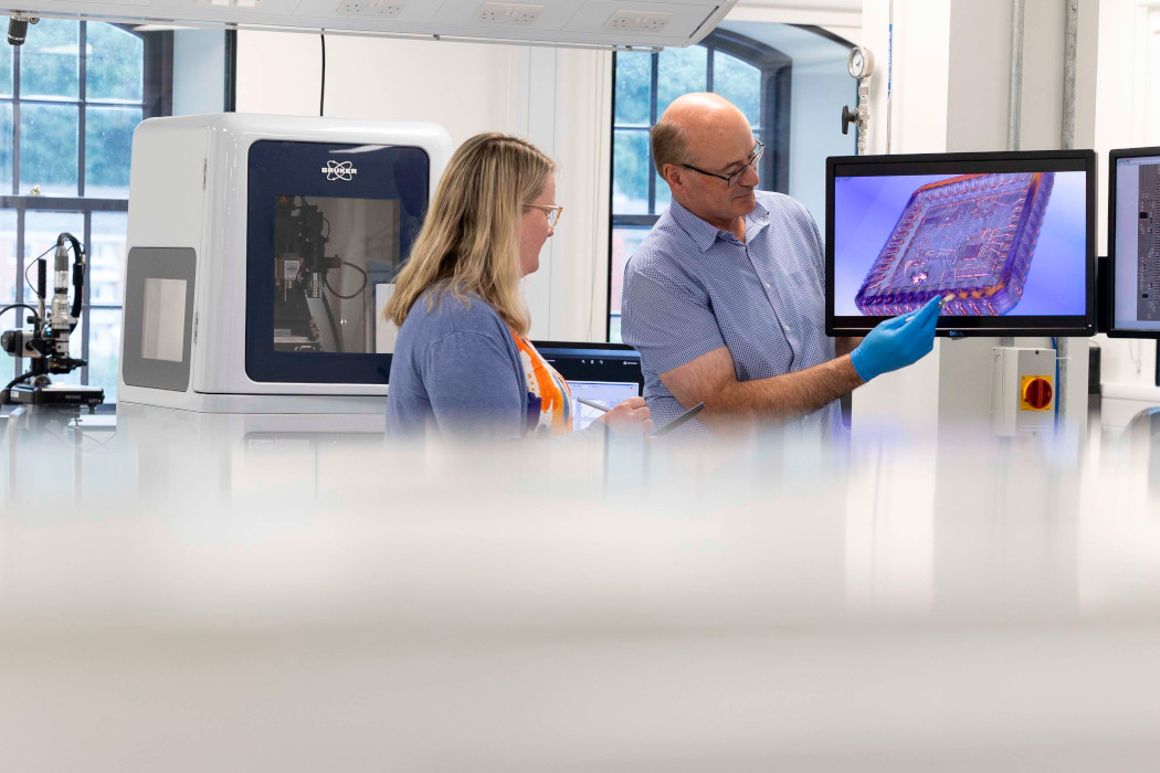
The services available from the team include
- Assembly of ICs and sensors in a wide variety of formats including – ceramic packages, chip-on-board, flip-chip & Multi-Chip Modules (MCMs)
- Development of customised packaging solutions & prototyping for specific applications
- Evaluation of new materials and technologies for use in high reliability applications
- Quality, reliability and failure analysis of all levels of packaging and interconnection
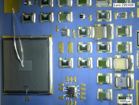
- Destructive and non-destructive physical analysis of components and PCB-based assemblies
- Environmental stress (reliability) testing up to space standards
The team has been involved in collaborative projects with leading industry clients for over 25 years and has been working with the European Space Agency (ESA) since 1998. All services are managed and provided in accordance with Tyndall’s ISO 9001:2015 quality system.
3D Virtual Lab Tour (Packaging and Component analysis)
3D Virtual Lab Tour (Relibility)
Electronics Packaging & Reliability Services
Electronics Packaging & Reliability Services
The Electronics Packaging and Reliability Services Team at Tyndall offers comprehensively equipped laboratories which specialise in the development of assembly & integration processes for Integrated Circuit and sensor devices. The team also offers expertise in valuation of assembly quality & reliability for standard and novel assemblies and a wide range of component analysis capabilities. The services available from the team include:
- Assembly of ICs and sensors in a wide variety of formats including – ceramic packages, chip-on-board, flip-chip & Multi-Chip Modules (MCMs).
- Development of customised packaging solutions & prototyping for specific applications.
- Evaluation of new materials and technologies for use in high reliability applications.
- Quality, reliability and failure analysis of all levels of packaging and interconnection.
- Destructive and non-destructive physical analysis of components and PCB-based assemblies.
- Environmental stress (reliability) testing up to space standards
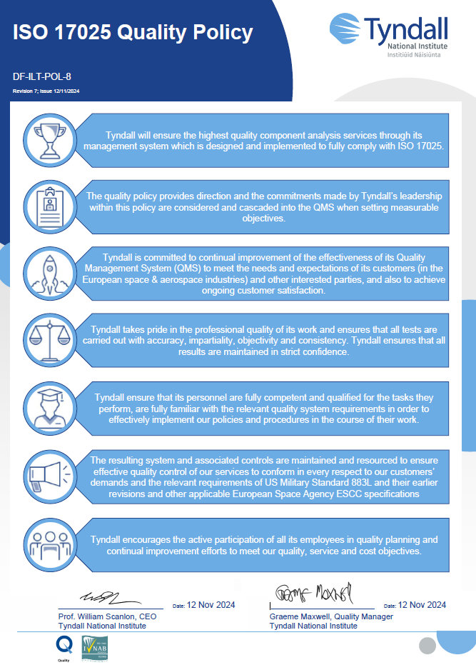
The team has been involved in collaborative projects with leading industry clients for over 25 years and has been working with the European Space Agency (ESA) since 1998. All services are managed & provided in accordance with Tyndall’s ISO 9001:2015 quality system, with space component DPA (Destructive Physical Analysis) services being accredited to ISO17025
Reliability Testing
The original environmental test facilities at Tyndall were established to provide testing for the European Space Agency, and can carry out testing to rigorous space standards. In recent years, a number of additional investments have helped to enhance the facility and have broadened the range of equipment so that a comprehensive suite of services can be offered. All of the principal test chambers can be automatically controlled from a central computer and biasing / monitoring of the devices under test can be carried out. The principal test facilities include:
- Air-to-air Thermal Shock Testing
- Temperature Cycling
- Temperature / Humidity Testing
- Burn-in Testing
- High & Low Temperature Storage Tests
- Vibration Testing (Swept Sinusoidal & Random Frequency).
- Mechanical Shock Testing
- Drop / Shock Testing
- Salt Spray Testing
- High temperature / vacuum storage
- Conditioning ovens.
The facilities in the reliability test laboratory are available to validate components and investigate the suitability of new technologies for possible use in space applications. The laboratory is managed by an experienced full-time engineer who has built up expertise in the definition of stress test programmes and the analysis of reliability test data.
Microelectronics & Microsystems Packaging
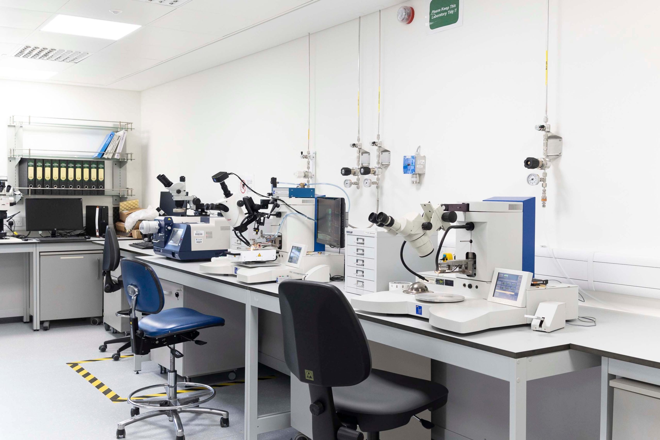
The Tyndall Microsystems Packaging Laboratory offers a comprehensive range of capabilities to support detailed component analysis work along with the packaging and assembly of microelectronics and microsystems components. The packaging operation supports the research work of Tyndall’s advanced research groups along with supporting the prototyping needs of Tyndall’s external client base including both industry users, project partners and the European Space Agency (ESA).
The packaging capability includes all of the processes required to take integrated circuits from the wafer and assemble them in a variety of packaged formats. The full packaging process available in the laboratory include: Ceramic Packaging, Chip-on-Board (CoB) assembly, Plastic (Glob-top) encapsulated assembly and Multi-Chip Module (MCM) assembly.
These processes are typically used in low-volume to build prototype devices for the validation of new technologies or the investigation of novel materials or assembly techniques. The facility supports the development of new IC & Microsystems technologies through the provision of a support service by which new devices may be quickly packaged for test and characterisation purposes.
The major packaging tools available in the laboratory include:
- Logitech PM5 lapping / grinding system (wafer & die thinning to < 100µm).
- 2 x Disco automatic dicing saws (wafers up to 8-inches / 200mm may be diced).
- Die ejection system (removal of individual ICs from dicing tape).
- Nordson EFD dispense system for die-attach & encapsulant dispense.
- Gold (Au) wire bonder.
- Aluminium (Al) 25µm wire bonder.
- Aluminium (Al) 150µm wire bonder for power packaging.
- Thermal & UV curing systems.
- To download details of wire bond process capabilities & design rules, click here.
Component Analysis
The Tyndall Microsystems Packaging Laboratory offers a comprehensive range of capabilities to support detailed component analysis work along with the packaging and assembly of microelectronics and microsystems components. The packaging operation supports the research work of Tyndall’s advanced research groups along with supporting the prototyping needs of Tyndall’s external client base including both industry users, project partners and the European Space Agency (ESA).
- Stereoscopic microscopes (equipped with digital cameras).
- Keyence VHX2000 3-Dimensional Optical Imaging System.
- High magnification metallurgical microscope (equipped with digital cameras).
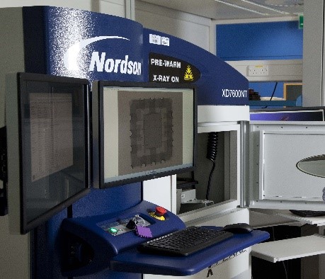
- Nordson Dage Diamond II XD7600 NT X-Ray Imaging System with µCT-Scan capability.
- Sonoscan D9600 Scanning Acoustic
- Microscope (SAM) equipped with a range of transducers (operating frequencies from 15MHz to 180MHz).
PTI Particle Impact Noise Detection (PIND) test system. - Trio Tech 481 series perfluorocarbon gross leak test system.
- Veeco MS18AB semi-automatic helium fine leak test system.
- Chemical & mechanical package decap.
- Microsectioning facilities (moulding, cutting, grinding & polishing to a 1µm finish).
- Solder baths (several available).
- Multicore MUST II solder wetting balance test system.
- Royce mechanical testers equipped with 20g & 50g wire bond pull cartridges and 20Kg component / die shear cartridge.
- Instron 5560 tensile and compressive mechanical test system equipped with 10N, 50N, 500N and 1,000N load cells
Accredited Space Component Destructive Physical Analysis (DPA) Service
Tyndall National Institute has a 30-year history working with the European Space Agency (ESA) on the quality & reliability evaluation of analysis flight-grade electronic components. Tyndall is now pleased to offer a Destructive Physical Analysis (DPA) service for space-grade electronic components which is fully accredited to ISO 17025.
The component DPA tests included in Tyndall’s Accreditation Scope are as follows:
- External Visual Inspection – Mil-Std-883L, Method 2009.14
- Radiography – Mil-Std-883L, Method 2012.11
- Seal – Helium Fine Leak Test – Mil-Std-883H, Method 1014.13, Condition A1
- Seal – Perfluorocarbon Gross Leak Test – Mil-Std 883L, Method 1014.17, Condition C1
- PIND (Particle Impact Noise Detection) Test – Mil-Std-883K, Method 2020.9, Condition A
- Internal Visual & SEM Inspection – Mil-Std-883L, Method 2013.1
- Wire Bond Pull Strength Test – Mil-Std-883L, Method 2011.10
- Die Shear Strength Test – Mil-Std-883L, Method 2019.10
