Developing low temperature and scalable processes for next generation materials is a central focus of the NanoIC pilot line. NanoIC brings together Europe’s leading research and technology organisations including imec (coordinator), CEA Leti, Fraunhofer Gesellschaft, VTT, CSSNT and Tyndall to create Europe’s most advanced open access pilot line for next generation integrated circuits. The initiative is a flagship action under the European Chips Act and is designed to strengthen Europe’s semiconductor supply chain and ensure global competitiveness.
As part of Tyndall’s contribution to the programme, researchers have published a new paper introducing a precise and low thermal budget method for engineering the 2D semiconductor molybdenum disulfide (MoS₂). The publication, titled “Low Temperature Site Specific Pulsed Laser Annealing of MoS₂“, demonstrates a localised laser annealing technique that enables controlled modification of MoS₂ while maintaining temperatures compatible with back end of line processing. This advancement directly supports the NanoIC technology roadmap, which identifies low temperature 2D processing and advanced material integration as key requirements for future device modules.
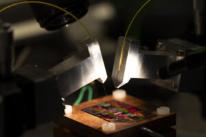
The research was carried out within NanoIC by Tyndall’s Aashi Gupta, Pavlina Metaxa, Ian Povey and Ray Duffy, in collaboration with the University of Galway. It forms part of Tyndall’s broader effort to develop pilot line ready materials and processes that can ultimately underpin new European semiconductor technologies.
This work also builds on expertise developed through the Research Ireland Frontiers for the Future Award “PLA2D”, a collaboration between Tyndall, the University of Galway, the University of Michigan and Imperial College London. The PLA2D programme has played a significant role in establishing Tyndall’s capabilities in TMD (Transition Metal Dichalcogenide) thin‑film device fabrication, capabilities that strengthened Tyndall’s successful bid to join the NanoIC pilot line. Since NanoIC’s launch, the two programmes have continued to benefit from complementary activities: NanoIC staff and students receive training from the PLA2D team, while PLA2D will gain enhanced capability through NanoIC’s planned investments in atomic‑layer processing and advanced characterisation.
Ray Duffy, Principal Researcher at Tyndall, commented:
This breakthrough shows how Tyndall’s research is directly advancing the NanoIC pilot line, enabling the low‑temperature 2D processing Europe needs for next‑generation semiconductor technologies.
The full publication is available here:
🔗 https://onlinelibrary.wiley.com/doi/10.1002/smll.202510617
The acquisition and operation of the NanoIC pilot line are jointly funded by the Chips Joint Undertaking, through the European Union’s Digital Europe programme (101183266) and Horizon Europe programme (101183277), as well as by the participating states Belgium (Flanders), France, Germany, Finland, Ireland and Romania. For more information, visit nanoic-project.eu.