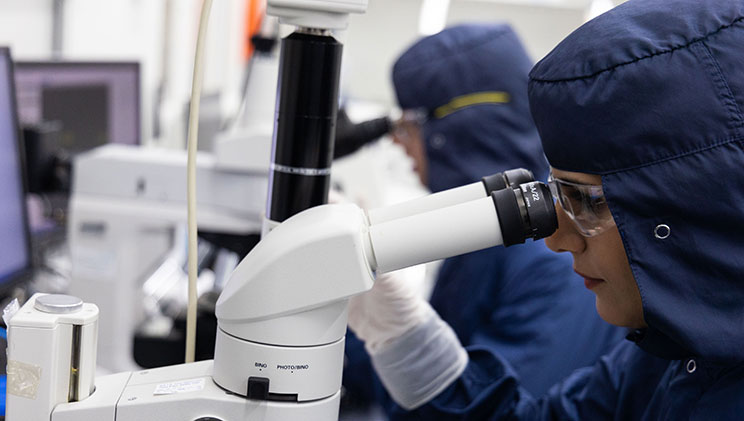
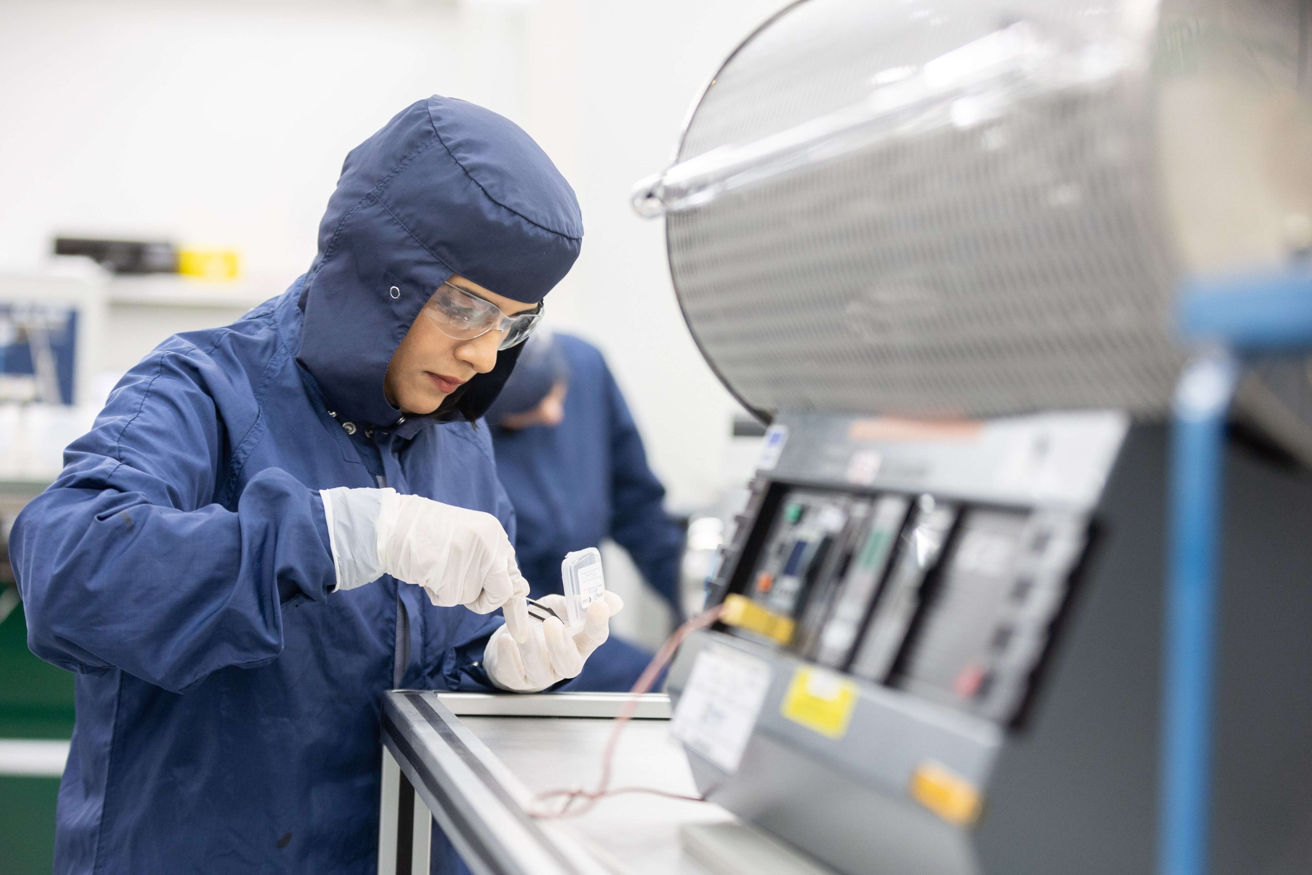
This website uses cookies Read More Ok
Leader in Integrated ICT Hardware & Systems

Virtual Lab Tours

Take a look inside a selection of laboratories at Tyndall National Institute.

Each virtual tour contains information about key pieces of equipment by simply clicking on the information icon to learn more.  

Packaging and Component Analysis Laboratory

The Tyndall Packaging and Component Analysis Laboratory offers a comprehensive range of capabilities to support detailed component analysis work along with the packaging and assembly of microelectronics and microsystems components.

The packaging operation supports the research work of Tyndall’s advanced research groups, along with supporting the prototyping needs of Tyndall’s external client base including both industry users, project partners and the European Space Agency (ESA).


Electrical Characterisation Laboratory

The Open Access Characterization Facility (OACF) is Tyndall's primary electrical test and wafer characterisation lab. The equipment contained herein allows wafer level analysis from -55 degrees Celsius to 300 degrees Celsius on wafers up to 200mm. The measurement accuracy levels that can be achieved allow analysis in the single Femto Amp and single Femto Farad range (Femto = 10e-15). The RF capability runs up to 110GHz (with higher analysis of specific harmonics also possible).

The OACF has MEMS analysis equipment using 2 Interferometers, and a Magnetic hysteresis capability allowing on chip analysis of magnetic components.
A recently acquired state of the art AFM (Atomic Force Microscope, a Bruker Dimension Icon) completes a suite of electrical characterisation equipment used by a broad range of researchers across multiple disciplines to facilitate Tyndall's ongoing world class research agenda.


Electron Beam Lithography Laboratory

The Elionix Electron Beam Lithography tool uses a direct writing technique that uses an accelerated beam of electrons to pattern features down to sub-10 nm on substrates that have been coated with an electron beam sensitive resist.

Exposure to the electron beam changes the solubility of the resist, enabling selective removal of either the exposed or non-exposed regions of the resist by immersing it in a developer.

Electron Microscopy Analysis Facility

The Electron Microscopy Analysis Facility (EMAF) Lab has the capabilities of combined Scanning Electron Microscope, Focussed Ion Beam systems in the areas of imaging, machining, material deposition and chemical analysis. The labs house state of the art 3 FIBs, 2 SEMs and a TEM managed by a team of experienced staff. 

The EMAF supports semiconductors testing, biological sample analysis, scientific research and development, inspection, failure investigation, and product development needs of Tyndall research groups and external client base with fast turnaround.

Training Fabrication Laboratory

Training fab is a dedicated facility at Tyndall which provides training courses for semiconductor device fabrication to internal and external students and professionals. The fab has all the required equipment to execute the practical side of the courses.

The equipment includes an eBeam evaporator, PECVD, thin film measurement, Mask Aligner, Rapid thermal processing, Cure oven, P10 Profiler, and microscope. During training, students get an overview and standard operating procedures for each tool in the lab.

III-V/MEMS Fabrication Laboratory

Tyndall has extensive wafer fabrication capabilities servicing III/V semiconductor devices, MEMs and CMOS compatible silicon processing. These capabilities span two separate cleanrooms – block C and block A cleanrooms.

These cleanrooms are also serviced by subfabs that house the necessary support equipment (gas supplies, de-ionised water generation and supply and waste treatment for example).

Tyndall SubFab Tour


Silicon Fabrication Laboratory

Silicon fab is a dedicated facility at Tyndall which provides semiconductor device fabrication to a wide range of customers, from students and researchers within Tyndall and educational institutions across Europe, to SME’s and multinational corporations. The fab has all the required equipment to produce CMOS devices on silicon and other compatible substrate materials (e.g. SOI, germanium etc.) with standard process-flows available for 1.5 µm / 5 µm gate-length transistors.

The equipment includes oxidation furnaces, lithography (stepper and mask-aligner), ion-implanter, dry-etch, PECVD, sputter and thin-film measurement. The fabrication facility is fully integrated with other key elements within Tyndall such as packaging, design, test and characterisation, electron microscopy and analysis. This provides our customers with a complete service solution from concept, circuit design, through to fabricated device, and packaged tested system. 


Reliability Test Laboratory

The Reliability Test Laboratory at Tyndall offers a range of environmental stress tests which can evaluate the reliability performance of electronic components and systems under severe operating conditions. The capabilities available include: air-to-air thermal shock testing; temperature cycling; temperature-humidity testing; high & low temperature storage testing; burn-in; mechanical shock & vibration tests. All of the tests can be carried out to  meet the  requirements of rigorous space test standards and are regularly used to evaluate components used in aerospace and other high-reliability applications – e.g. telecommunications, automotive and medical systems.