The Scanning Electron Microscope (SEM) allows Physicists to picture the universe resulting in some exciting images. Outputs of a detector (voltage) transformed in intensity grey scale are a real expression of science and art. These images can be showcased in their original form and further enhanced with the use of false colours. For World Quantum Day 2023, we are highlighting some of Tyndall’s science images in Quantum Physics.
Quantum dots (QD’s) are small 3D structures (tens of nm in size or less) which can emit “quantum light”, specifically entangled light when optically excited. Tyndall’s work concentrates on site-control i.e. on dot structures which form in recesses after Gallium Arsenide (GaAs) wafers are lithographically processed with inverted pyramidal recesses. While in general, a single quantum dot is deposited at the centre of the recess by metalorganic vapour phase epitaxy (MOVPE), one can also stack several, either to design new quantum dot devices and emitters, or to study their structural properties. In the image Pyramidal Dots (Fig 1), we present some representative microscopy images in their original greyscale, showing a number of interesting features (see also Holsgrove, Kristina M., et al. "Towards 3D characterisation of site-controlled InGaAs pyramidal QDs at the nanoscale." Journal of Materials Science 57.34 (2022): 16383-16396).

Stacked site-controlled Pyramidal quantum dot structures are shown in: a) combined SEM image showing a typical single dot structure after metalorganic vapour phase epitaxy; b) HAADF STEM overview image indicating the number of QDs: 1 – 9. Here the microscopy image is taken in cross section and shows quantum dots in the centre connected to lateral quantum wires; c) HAADF STEM overviews of the plan view sample, i.e. the image is taken from the top after sample polishing, and shows the formation of hexagonally shaped quantum dots at the centre. The grey images are exactly as they emerge under the microscope, and the semiconductor material is AlGaAs, of which we have layers of different Aluminum content (down to zero) and InGaAs quantum dots. The darker regions indicatively signify layers of the semiconductor structure which are richer in aluminium, while GaAs and InGaAs appear lighter. We caution the reader that the signal detected in electron microscopes can vary significantly due to several variables, and the grey scale gives qualitative information only about the semiconductor alloy composition.
Greyscale images are ideal in instances where viewers can clearly delineate each component of information from an image. In other situations where images are less coherent, there is a need to provide further information by using false colours.
The Scanning Electron Microscope images (Nano-gate Highway and GeSn Coral Beach) are related to a collaborative work between Munster Technological University and Tyndall National Institute in engineering of quantum devices, manufactured using the same complementary metal-oxide-semiconductor (CMOS) very large-scale integration (VLSI) technologies underpinning today’s semiconductor industry. While it is becoming increasingly evident that Si can be an excellent host material for an entirely new generation of devices, based on the quantum properties of charges and spins, the building blocks of a quantum processor can largely benefit by another group IV material such as Ge and its alloys with Sn.
In the Nano-gate Highway SEM image we replaced the usual greyscale with false colours to enhance the main topologies of 30 nm gate arrays used to define quantum dots in the underlaying Ge substrate.

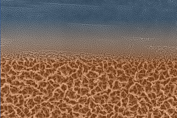
The false colours on the SEM image called GeSn Coral Beach, provide artistic representation of a problem with the Ge-based substrates when irradiated with a Ga-ion focused ion beam (FIB) used for preparing samples for transmission electron microscopy imaging (TEM). The surface defects observed after irradiation resemble nano-scaled Coral Beach but their origin is explained by Ga-ion irradiation induced surface texturing related to crystal damage accumulation in the underlying substrate.

Physicists endeavour to generate meaningful interpretations of the quantum realm which is intrinsically fuzzy and probabilistic. Using SEM images and adapting them with the use of false colours allows physicists to uncover properties and behaviours occurring at the smallest of scales, within the very basic building blocks of nature.
For more information about World Quantum Day, head to: https://worldquantumday.org/