Congratulations to the winners of the STS Elionix Scientific Image competition of Q3 2022!
The STS Elionix Scientific Image competition allows us to showcase the creative side of the researchers here at Tyndall. They share scientific images from their research which they have discovered to be visually striking or informative to the technically excellent.
The judges for the Q3 competition were Prof. William Scanlon, CEO; Peter Smyth, Commercial Director; Ursula Morrish, Marketing & Communications Manager; Graeme Maxwell, Head of Specialty Products & Services; and Dr Daniela Iacopino, Researcher, MNS.
The exceptional quality and creativity in the four images led to the votes being cast to the following winners: Cathal Larrigy (The Great Wave of LIG), Davinder Singh (Mosaic in Crystals), Nikolay Petkov, Sinan Bugu, Ray Duffy, Giorgos Fagas (Nano-Highway) and Lorraine Nagle (Trigonal Pyramids).
The winners are each awarded a €100 Me2You Gift Card, kindly sponsored by STS Elionix.
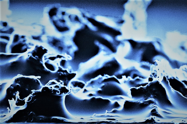
The Great Wave of LIG
Cathal Larrigy, Nanotechnology Group

Laser-induced graphene (LIG) is a method by which the fabrication of 3D, porous conductive, carbon structures with high surface area can be constructed via laser-irradiation of a target substrate. Typically, LIG is fabricated on non-sustainable feedstock substrates, most commonly polyimide. Alternatively, our projects aim to fabricate LIG on more sustainable substrates.
This image is a scanning electron micrograph of a cross section of laser-induced graphene fabricated on a chitosan-based bioplastic. Chitosan is the acetylated form of chitin, the main component of most hard shell and exoskeleton containing wildlife, such as shrimp, crabs, and insects. As such, it is often cited as the second most abundant polysaccharide. Chitosan is formulated into a chitosan-based bioplastic composite, and a simple 3-step laser fabrication process additively converts the chitosan-based bioplastic composite into LIG.
SEMs of LIG allow for examination of LIGs surface 3D micro/nano porous morphology. The micrograph was edited with blue hue, as it represents a striking similarity with the artist Hokusai's work, “The Great Wave off the Coast of Kanagawa”.
Mosaic in Crystals
Davinder Singh, EMAF

This image shows diffraction patterns of Gold, also called Kikuchi pattern, named after the scientist who came up with the theory.
Japanese physicist, Seishi Kikuchi, first explained the phenomena of electron backscattered diffraction in crystalline materials, leading to such mosaic patterns. These patterns are only observed in crystalline materials like metals, alumina, quartz, diamond and more importantly table salt and sugar.
Based on the above phenomena, Electron Backscatter Diffraction (EBSD) technique was developed, which enables a sample’s microstructure to be analysed using scanning electron microscope. This technique is extensively used in the fields of aerospace, earth sciences, metallurgy and nuclear science.
In the image Kikuchi pattern of Gold has been obtained on Tyndall's newly acquired Plasma FIB-SEM. This microscope has ultra-high-resolution imaging capability coupled with Oxford EBSD detector. This will enable researchers to perform crystallographic study of their samples, along with existing elemental analysis available at Tyndall EMAF Labs.
Nano-Highway
Nikolay Petkov, Sinan Bugu, Ray Duffy and Giorgos Fagas, CMOS++

This image shows a new building block for quantum sensors based on quantum nano-mechanical resonator devices, fabricated at Tyndall in the Block A cleanroom.
It is becoming increasingly evident that Si can be an excellent host material for an entirely new generation of devices, based on the quantum properties of charges and spins. The building block of a quantum processor is the quantum bit (qubit). In Si-based quantum devices, the qubit is formed by the spin degree of freedom of a charge carrier (electron or hole) trapped in quantum dots.
As Si qubit devices are Si nanowire in form we are able to fabricate qubit sensors, based on a nano-mechanical resonator design, on the same mask as the qubits.
The key difference is that the sensor devices have no gate electrode. Devices are typically characterised by electrical transport measurements biased across temperatures and frequencies.
Trigonal Pyramids
Lorraine Nagle, Electrochemical Materials and Energy group

A facile route to generating trigonal pyramidal copper oxide microcrystals, captured in the plan view SEM image, was identified during the competitive electrodeposition and dissolution of copper in an acidic copper plating bath.
The facet-controlled synthetic pathway was revealed in this EU-funded CuBER research project (Copper-based flow Batteries for Energy storage Renewables integration).
The trigonal pyramids grow from an equilateral, scalar or isosceles triangular base and are bound by three lateral sides. Shape control of metallic particles receives considerable attention due to their unique facet-dependent electronic, magnetic, optical, and catalytic properties which have a wide range of applications including chemical and bio-sensing, catalysis, photonics, and optoelectronics. In the particular case of copper oxide nanocrystals, their surface facet-dependent properties have been exploited in gas catalysis, photocatalysis, organocatalysis and sensing applications.